Wednesday, 26 February 2014

Week 4

This week, we first compared the voltage transfer curves of CMOS of different electron and holes mobilities and then change the aspect ratio of enhancement load MOSFET to inspect the differences between curves. The same processes are taken as the last week. The ratio of the mobility in proportional to the aspect ratio. 


For the organic CMOS, the code can be shown as

The result can be shown as:

Explanation:

In silicon semiconductors, the mobility of electron(un) is twice of the mobility of holes. On the other hand, holes mobility is the double of electron mobility in organic semiconductors. The final voltage transfer curves of two kind of transistors are shown in the figure above. It can be observed that there is a shift between two curves. That is to say, when the nMOS and pMOS both saturate, the input voltage of silicon transistor is smaller than the input voltage of organic transistor.

It is known that, with the increase of input voltage, the pMOS goes from linear region into saturation region. Since the nMOS saturates after Vin is larger then Vtn, once the pMOS saturates, both parts saturate. At that input voltage value, the curve falls sharply and seems to be a straight line that perpendicular to the x axis. Because nMOS and pMOS are both saturates, that particular value of input voltage can be derived as:
In this simulation, the aspect ratio does not change and mobility of holes and electrons differs between silicon and organic transistors. Hence \beta n/\beta p is un/up, which means the special input voltage is decided by the mobility. Since un/up in organic CMOS is 2 and in silicon is 0.5, the voltage value of organic is larger than silicon. That explain why there is a shift between two curves.


The code for researching the mobility effects on the PMOS can be shown as:
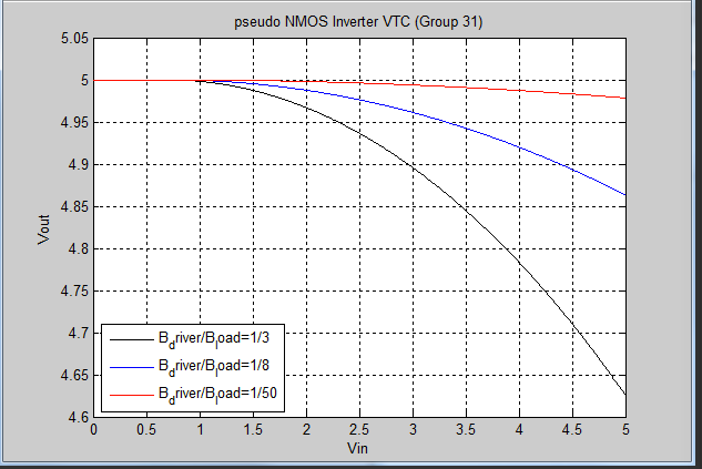
The result that we got :

Explanation:

For a enhancement load n channel MOS, the load transistor gate is connected to the drain, 
hence the load is always saturated. When the input voltage applied to the driver transistor is less than Vtdriver, the output voltage is the voltage across load, that is VDD-Vtload.
When input voltage grows larger than Vtdriver, the driver is also saturated and a drain current is induced in to driver transistor. At that region, the output voltage is linear with input voltage. As the input voltage further increases, the driver transistor no longer saturated but the driver and load drain currents are still equal. As a result, the input-output relationship is a curve rather than a straight line. The aspect ratio decides the slope in the driver-saturation region, thus when the aspect ratio increase the line of input-output falls sharper. In addition, when the aspect ratio decreases, the effective resistance increases, hence the minimum output voltage decreases.

Monday, 17 February 2014

Week 3

This week, we did further research on organic CMOS and PMOS.

According to the supervisor's suggestion, we need to use MATLAB to simulate the voltage transfer characteristics curves of organic CMOS and PMOS. 

1. Organic CMOS VTC
we try to use MATLAB to simulate the voltage transfer characteristics curve of the organic CMOS. Some parameters are given by the supervisor, which are shown as following.
The hole mobility,up, is given as: 0.0001(m^2)/vs
The electron mobility, un, is given as 0.00005(m^2)/vs
The oxide capacitance, Cox, is 1.66*(10^-4) f/(m^2).

In MOSFET, K is a very important parameter which is known as transistor conduction parameter. Kn is for NMOS and Kp is for PMOS.

where un is electron mobility, up is hole mobility and Cox is oxide capacitance.
Moreover, Cox is given by
where tox is oxide thichness and εox is oxide permittivity, which is given by
Furthermore, k'n and k'p are process conduction parameter. In this case,
k'n=0.0001(m^2)/vs*1.66*(10^-4) f/(m^2)=1.66*10^-9 F/vs
k'p=0.00005(m^2)/vs*1.66*(10^-4) f/(m^2)=8.3*10^-9 F/vs


Then, we use the MATLAB to draw the curve. The code can be shown as :
 The curve can be shown as:

In order to find the different conditions in different aspect ratios. The code can be changed as:

Then the curve can be drawn as:


2 PMOS VTC

A pseudo PMOS circuit should be like 
for a PMOS, VDD should be -VDD and VDS, VGS should be VSD and VSG.

(1)When Vin < VTD,
driver is cut off and the currents are zero. Hence the maximum output voltage does not reach the full VDD value:
(2)When Vin>VTD,
driver transistor turns on and is biased in the saturation region.
The output voltage can be given as:
The output voltage decreases linearly with Vin.

(3)When Vin>VIt,
Input voltage at the transition point is given as:

When input voltage is larger than VIt, the driver becomes biased in the non-saturation region, and then
The relationship between input voltage and output voltage is no longer linear.

The last VTC should be like

When the aspect ratio is greater than unity, the inverter gain magnitude is greater than unity.
The W/L for load is given as 15um/5um while the W/L for driver is 5um/5um,while changing aspect ratio to other values, the curve can be drawn as:


The code for this process is shown as:


Friday, 7 February 2014

Week 2

This week, we studied the voltage transfer characteristics of CMOS and PMOS, which can be treated as the basic knowledge of the organic CMOS and PMOS research.

According to the supervisor's suggestion, we use MATLAB to simulate the voltage transfer characteristics of CMOS and pseudo-NMOS in different aspect ratio.


CMOS inverter
The voltage transfer curve of a CMOS can be divided into 5 regions.

Region 1 ( 0≤ Vin < VTN ):
Pull Down Network (PDN, n-channel) is cut off, hence the Vout is pulled to VDD, Vout = VDD

Region 2 ( VTN≤Vin<Vo一|VTP|):
PDN is in saturation, PUN(Pull up net work, PMOS) is in triode. At this time, the current in PDN is
The current in PUN should be
and these two currents should be euqal in a no-load CMOS inverter.
Thus, the Vout is

Region 4 (Vout + VTN ≤ Vin <VDD - |VTP|):

PDN is in triode, PUN is in saturation.
The current in PUN should be

The current in PDN should be
and these two currents should be equal in a no-load CMOS inverter.
Hence, the Vout is
Region 5 (Vin> VDD -|VTP|):
PUN is off, hence the Vout=0.


The basic code for the COMS VTC can be shown as


In addition, the curve can be shown as


Then, experiments should change the aspect ratio of the P-Channel (PMOS) and N-Channel (NMOS) to observe the change of the voltage transfer characteristics curve. Therefore, the MATLAB code can be changed in below:


Also, the curve can be found as


Pseudo-NMOS
In a pseudo-NMOS, the pull up network is replaced with a single unconditional load device--a single PMOS transistor whose gate is grounded, which means that t is always on. The pull down network is still a NMOS.

The currents in the pseudo-NMOS under different Voltage conditions:
NMOS current:
PMOS current:
Pseudo-NMOS's voltage curve can be divided into 4 regions:
Region 1 (vi < Vtn):
Vout= VDD
Region 2 (vO ≥ vi-Vtn vO ≥ |Vtp|):
Region 3 (vO ≥ vi-Vtn vO < |Vtp|):
This is a short segment that is not of great interest.
Region 4 (vO < vi-Vtn vO < |Vtp|):
and in this region, the voltage will eventually decrease to  VOL:
(r is aspect ratio βN/βP)


The MATLAB code can be shown as:


The curve can be found as:

The red curve is r=100, the blue one is r=8 and the black is r=4.
The curves share the similar shape which is also the shape of a normal CMOS inverter. However, the VOL increases when the ratio of βN/βP decreases and for a large βN/βP, the VOL approaches 0. Hence, it is clear that pseudo NMOS is a type of ratioed logic, where relative device sizes set VOL or VOH.